Interface Serial Spi


SPI bus: single master and single slave
The Serial Peripheral Interface SPI bus is a synchronous serial communication interface specification used for short distance communication, primarily in embedded systems. The interface was developed by Motorola and has become a de facto standard. Typical applications include sensors, Secure Digital cards, and liquid crystal displays.
SPI devices communicate in full duplex mode using a master-slave architecture with a single master. The master device originates the frame for reading and writing. Multiple slave devices are supported through selection with individual slave select SS lines.
Sometimes SPI is called a four-wire serial bus, contrasting with three-, two-, and one-wire serial buses. The SPI may be accurately described as a synchronous serial interface, 1 but it is different from the Synchronous Serial Interface SSI protocol, which is also a four-wire synchronous serial communication protocol, but employs differential signaling and provides only a single simplex communication channel.
2.4 Independent slave configuration
2.8 Example of bit-banging the master protocol
7.1 Intelligent SPI controllers
7.7 Intel Enhanced Serial Peripheral Interface Bus
The SPI bus specifies four logic signals:
SCLK : Serial Clock output from master.
MOSI : Master Output, Slave Input output from master.
MISO : Master Input, Slave Output output from slave.
SS : Slave Select active low, output from master.
Alternative naming conventions are also widely used, and SPI port pin names for particular IC products may differ from those depicted in these illustrations:
MOSI : SIMO, SDI for slave devices, DI, DIN, SI, MTST.
MISO : SOMI, SDO for slave devices , DO, DOUT, SO, MRSR.
SS : nCS, CS, CSB, CSN, EN, nSS, STE, SYNC.
The MOSI/MISO convention requires that, on devices using the alternate names, SDI on the master be connected to SDO on the slave, and vice versa. Chip select polarity is rarely active high, although some notations such as SS or CS instead of nSS or nCS suggest otherwise. Slave select is used instead of an addressing concept.
The SPI bus can operate with a single master device and with one or more slave devices.
If a single slave device is used, the SS pin may be fixed to logic low if the slave permits it. Some slaves require a falling edge of the chip select signal to initiate an action, an example is the Maxim MAX1242 ADC, which starts conversion on a high low transition. With multiple slave devices, an independent SS signal is required from the master for each slave device.
Most slave devices have tri-state outputs so their MISO signal becomes high impedance logically disconnected when the device is not selected. Devices without tri-state outputs cannot share SPI bus segments with other devices; only one such slave could talk to the master.
A typical hardware setup using two shift registers to form an inter-chip circular buffer
To begin communication, the bus master configures the clock, using a frequency supported by the slave device, typically up to a few MHz. The master then selects the slave device with a logic level 0 on the select line. If a waiting period is required, such as for analog-to-digital conversion, the master must wait for at least that period of time before issuing clock cycles.
During each SPI clock cycle, a full duplex data transmission occurs. The master sends a bit on the MOSI line and the slave reads it, while the slave sends a bit on the MISO line and the master reads it. This sequence is maintained even when only one-directional data transfer is intended.
Transmissions normally involve two shift registers of some given word size, such as eight bits, one in the master and one in the slave; they are connected in a virtual ring topology. Data is usually shifted out with the most-significant bit first, while shifting a new least-significant bit into the same register. After that register has been shifted out, the master and slave have exchanged register values. If more data needs to be exchanged, the shift registers are reloaded and the process repeats. Transmission may continue for any number of clock cycles. When complete, the master stops toggling the clock signal, and typically deselects the slave.
Transmissions often consist of 8-bit words. However, other word sizes are also common, for example, 16-bit words for touchscreen controllers or audio codecs, such as the TSC2101 by Texas Instruments, or 12-bit words for many digital-to-analog or analog-to-digital converters.
Every slave on the bus that has not been activated using its chip select line must disregard the input clock and MOSI signals, and must not drive MISO. The master must select only one slave at a time.
A timing diagram showing clock polarity and phase. The red vertical line represents CPHA 0 and the blue vertical line represents CPHA 1
In addition to setting the clock frequency, the master must also configure the clock polarity and phase with respect to the data. Freescale s SPI Block Guide 2 names these two options as CPOL and CPHA respectively, and most vendors have adopted that convention.
The timing diagram is shown to the right. The timing is further described below and applies to both the master and the slave device.
At CPOL 0 the base value of the clock is zero
For CPHA 0, data are captured on the clock s rising edge low high transition and data is propagated on a falling edge high low clock transition.
For CPHA 1, data are captured on the clock s falling edge and data is propagated on a rising edge.
At CPOL 1 the base value of the clock is one inversion of CPOL 0
For CPHA 0, data are captured on clock s falling edge and data is propagated on a rising edge.
For CPHA 1, data are captured on clock s rising edge and data is propagated on a falling edge.
That is, CPHA 0 means sample on the leading first clock edge, while CPHA 1 means sample on the trailing second clock edge, regardless of whether that clock edge is rising or falling. Note that with CPHA 0, the data must be stable for a half cycle before the first clock cycle.
The MOSI and MISO signals are usually stable at their reception points for the half cycle until the next clock transition. SPI master and slave devices may well sample data at different points in that half cycle.
This adds more flexibility to the communication channel between the master and slave.
The combinations of polarity and phases are often referred to as modes which are commonly numbered according to the following convention, with CPOL as the high order bit and CPHA as the low order bit:
For Microchip PIC / ARM-based microcontrollers note that NCPHA is the inversion of CPHA :
For PIC32MX : SPI mode configure CKP,CKE and SMP bits.Set SMP bit,and CKP,CKE two bits configured as above table.
Another commonly used notation represents the mode as a CPOL, CPHA tuple; e.g., the value 0, 1 would indicate CPOL 0 and CPHA 1.
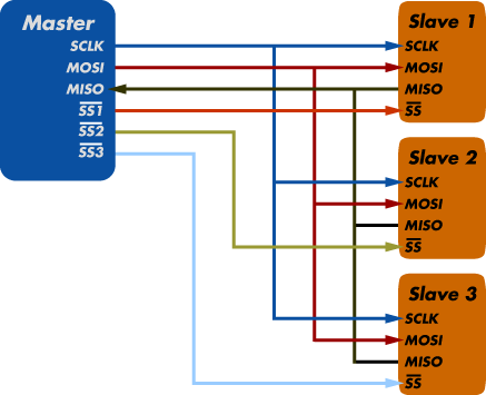
Independent slave configuration edit
Typical SPI bus: master and three independent slaves
In the independent slave configuration, there is an independent chip select line for each slave. This is the way SPI is normally used. Since the MISO pins of the slaves are connected together, they are required to be tri-state pins high, low or high-impedance.
Daisy chain configuration edit
Daisy-chained SPI bus: master and cooperative slaves
Some products that implement SPI may be connected in a daisy chain configuration, the first slave output being connected to the second slave input, etc. The SPI port of each slave is designed to send out during the second group of clock pulses an exact copy of the data it received during the first group of clock pulses. The whole chain acts as a communication shift register; daisy chaining is often done with shift registers to provide a bank of inputs or outputs through SPI. Such a feature only requires a single SS line from the master, rather than a separate SS line for each slave. 3
Applications that require a daisy chain configuration include SGPIO and JTAG.
Some slave devices are designed to ignore any SPI communications in which the number of clock pulses is greater than specified. Others do not care, ignoring extra inputs and continuing to shift the same output bit. It is common for different devices to use SPI communications with different lengths, as, for example, when SPI is used to access the scan chain of a digital IC by issuing a command word of one size perhaps 32 bits and then getting a response of a different size perhaps 153 bits, one for each pin in that scan chain.
SPI devices sometimes use another signal line to send an interrupt signal to a host CPU. Examples include pen-down interrupts from touchscreen sensors, thermal limit alerts from temperature sensors, alarms issued by real time clock chips, SDIO, 4 and headset jack insertions from the sound codec in a cell phone. Interrupts are not covered by the SPI standard; their usage is neither forbidden nor specified by the standard.
Example of bit-banging the master protocol edit
Below is an example of bit-banging the SPI protocol as an SPI master with CPOL 0, CPHA 0, and eight bits per transfer. The example is written in the C programming language. Because this is CPOL 0 the clock must be pulled low before the chip select is activated. The chip select line must be activated, which normally means being toggled low, for the peripheral before the start of the transfer, and then deactivated afterwards. Most peripherals allow or require several transfers while the select line is low; this routine might be called several times before deselecting the chip.
Simultaneously transmit and receive a byte on the SPI.
Polarity and phase are assumed to be both 0, i.e.:
- input data is captured on rising edge of SCLK.
- output data is propagated on falling edge of SCLK.
uint8_t SPI_transfer_byte uint8_t byte_out
/ Shift-out a bit to the MOSI line /
write_MOSI byte_out bit . HIGH : LOW ;
/ Delay for at least the peer s setup time /
/ Shift-in a bit from the MISO line /
/ Delay for at least the peer s hold time /
Full duplex communication in the default version of this protocol.
Push-pull drivers as opposed to open drain provide good signal integrity and high speed
Higher throughput than I C or SMBus
Complete protocol flexibility for the bits transferred
Arbitrary choice of message size, content, and purpose
Extremely simple hardware interfacing
Typically lower power requirements than I C or SMBus due to less circuitry including pull up resistors
No arbitration or associated failure modes
Slaves use the master s clock, and do not need precision oscillators
Slaves do not need a unique address unlike I C or GPIB or SCSI
Uses only four pins on IC packages, and wires in board layouts or connectors, much fewer than parallel interfaces
At most one unique bus signal per device chip select ; all others are shared
Signals are unidirectional allowing for easy Galvanic isolation
Not limited to any maximum clock speed, enabling potentially high speed
Requires more pins on IC packages than I C, even in the three-wire variant
No in-band addressing; out-of-band chip select signals are required on shared buses
No hardware flow control by the slave but the master can delay the next clock edge to slow the transfer rate
No hardware slave acknowledgment the master could be transmitting to nowhere and not know it
Supports only one master device
No error-checking protocol is defined
Without a formal standard, validating conformance is not possible
Only handles short distances compared to RS-232, RS-485, or CAN-bus
Many existing variations, making it difficult to find development tools like host adapters that support those variations
SPI does not support hot swapping dynamically adding nodes.
Interrupts must either be implemented with out-of-band signals or be faked by using periodic polling similarly to USB 1.1 and 2.0
Some variants like Multi I/O SPI and three-wire serial buses defined below are half-duplex.
The board real estate savings compared to a parallel I/O bus are significant, and have earned SPI a solid role in embedded systems. That is true for most system-on-a-chip processors, both with higher end 32-bit processors such as those using ARM, MIPS, or PowerPC and with other microcontrollers such as the AVR, PIC, and MSP430. These chips usually include SPI controllers capable of running in either master or slave mode. In-system programmable AVR controllers including blank ones can be programmed using an SPI interface. 5
Chip or FPGA based designs sometimes use SPI to communicate between internal components; on-chip real estate can be as costly as its on-board cousin.
The full-duplex capability makes SPI very simple and efficient for single master/single slave applications. Some devices use the full-duplex mode to implement an efficient, swift data stream for applications such as digital audio, digital signal processing, or telecommunications channels, but most off-the-shelf chips stick to half-duplex request/response protocols.
SPI is used to talk to a variety of peripherals, such as
Sensors: temperature, pressure, ADC, touchscreens, video game controllers
Control devices: audio codecs, digital potentiometers, DAC
Camera lenses: Canon EF lens mount
Communications: Ethernet, USB, USART, CAN, IEEE 802.15.4, IEEE 802.11, handheld video games
LCD, sometimes even for managing image data
Any MMC or SD card including SDIO variant 4
For high performance systems, FPGAs sometimes use SPI to interface as a slave to a host, as a master to sensors, or for flash memory used to bootstrap if they are SRAM-based.
JTAG is essentially an application stack for a three-wire SPI flavor, using different signal names: citation needed TCK not SCK, TDI not MOSI, TDO not MISO. It defines a state machine driven by a TMS signal instead of a chip select line, protocol messages, a core command set, the ability to daisy-chain devices in a scan chain, and how vendors define new commands. The devices in a scan chain are initially treated as a single device, and transitions on TMS update their state machines; once the individual devices are identified, commands may be issued that affect only one device in that scan chain. Different vendors use different JTAG connectors. Bit strings used in JTAG are often long and not multiples of 8 bit words; for example, a boundary scan reports signal state on each of several hundred pins.
SGPIO is essentially another incompatible application stack for SPI designed for particular backplane management activities. citation needed SGPIO uses 3-bit messages.
The SPI bus is a by default standard. However, the lack of a formal standard is reflected in a wide variety of protocol options. Different word sizes are common. Every device defines its own protocol, including whether or not it supports commands at all. Some devices are transmit-only; others are receive-only. Chip selects are sometimes active-high rather than active-low. Some protocols send the least significant bit first.
Some devices even have minor variances from the CPOL/CPHA modes described above. Sending data from slave to master may use the opposite clock edge as master to slave. Devices often require extra clock idle time before the first clock or after the last one, or between a command and its response. Some devices have two clocks, one to read data, and another to transmit it into the device. Many of the read clocks run from the chip select line.
Some devices require an additional flow control signal from slave to master, indicating when data are ready. This leads to a 5-wire protocol instead of the usual 4. Such a ready or enable signal is often active-low, and needs to be enabled at key points such as after commands or between words. Without such a signal, data transfer rates may need to be slowed down significantly, or protocols may need to have dummy bytes inserted, to accommodate the worst case for the slave response time. Examples include initiating an ADC conversion, addressing the right page of flash memory, and processing enough of a command that device firmware can load the first word of the response. Many SPI masters do not support that signal directly, and instead rely on fixed delays.
Many SPI chips only support messages that are multiples of 8 bits. Such chips can not interoperate with the JTAG or SGPIO protocols, or any other protocol that requires messages that are not multiples of 8 bits.
There are also hardware-level differences. Some chips combine MOSI and MISO into a single data line SI/SO ; this is sometimes called three-wire signaling in contrast to normal four-wire SPI. Another variation of SPI removes the chip select line, managing protocol state machine entry/exit using other methods. Anyone needing an external connector for SPI defines their own: UEXT, JTAG connector, Secure Digital card socket, etc. Signal levels depend entirely on the chips involved.
SafeSPI is an industry standard for SPI in automotive applications. Its main focus is the transmission of sensor data between different devices.
When developing or troubleshooting systems using SPI, visibility at the level of hardware signals can be important.
There are a number of USB hardware solutions to provide computers, running Linux, Mac, or Windows, SPI master and/or slave capabilities. Many of them also provide scripting and/or programming capabilities Visual Basic, C/C, VHDL etc..
An SPI host adapter lets the user play the role of a master on an SPI bus directly from PC. They are used for embedded systems, chips FPGA/ASIC/SoC and peripheral testing, programming and debugging.
The key parameters of SPI adapters are: the maximum supported frequency for the serial interface, command-to-command latency and the maximum length for SPI commands. It is possible to find SPI adapters on the market today that support up to 100 MHz serial interfaces, with virtually unlimited access length.
SPI protocol being a de facto standard, some SPI host adapters also have the ability of supporting other protocols beyond the traditional 4-wires SPI for example, support of quad-SPI protocol or other custom serial protocol that derive from SPI 6.
Examples of SPI adapters manufacturers in alphabetical order :
I C, SPI, single, dual and quad
SPI protocol analyzers are tools which sample an SPI bus and decode the electrical signals to provide a higher-level view of the data being transmitted on a specific bus.
Examples of SPI protocol analysers manufacturers in alphabetical order :
Analogue 50 Mega-samples/second
Every major oscilloscope vendor offers oscilloscope-based triggering and protocol decoding for SPI. Most support 2-, 3-, and 4-wire SPI. The triggering and decoding capability is typically offered as an optional extra. SPI signals can be accessed via analog oscilloscope channels or with digital MSO channels. 7
When developing and/or troubleshooting the SPI bus, examination of hardware signals can be very important. Logic analyzers are tools which collect, analyze, decode, and store signals so people can view the high-speed waveforms at their leisure. Logic analyzers display time-stamps of each signal level change, which can help find protocol problems. Most logic analyzers have the capability to decode bus signals into high-level protocol data and show ASCII data.
Intelligent SPI controllers edit
A queued serial peripheral interface QSPI is a type of SPI controller that uses a data queue to transfer data across the SPI bus. 8 It has a wrap-around mode allowing continuous transfers to and from the queue with only intermittent attention from the CPU. Consequently, the peripherals appear to the CPU as memory-mapped parallel devices. This feature is useful in applications such as control of an A/D converter. Other programmable features in QSPI are chip selects and transfer length/delay.
SPI controllers from different vendors support different feature sets; such DMA queues are not uncommon, although they may be associated with separate DMA engines rather than the SPI controller itself, such as used by multichannel buffered serial port MCBSP. 9 Most SPI master controllers integrate support for up to four chip selects, 10 although some require chip selects to be managed separately through GPIO lines.
Microwire, 11 often spelled μWire, is essentially a predecessor of SPI and a trademark of National Semiconductor. It s a strict subset of SPI: half-duplex, and using SPI mode 0. Microwire chips tend to need slower clock rates than newer SPI versions; perhaps 2 MHz vs. 20 MHz. Some Microwire chips also support a three-wire mode, which fits neatly with the restriction to half-duplex.
Microwire/Plus 12 is an enhancement of Microwire and features full-duplex communication and support for SPI modes 0 and 1. There was no specified improvement in serial clock speed.
As mentioned, one variant of SPI uses single bidirectional data line slave out/slave in, called SISO instead of two unidirectional ones MOSI and MISO. This variant is restricted to a half duplex mode. It tends to be used for lower performance parts, such as small EEPROMs used only during system startup and certain sensors, and Microwire. Few SPI master controllers support this mode; although it can often be easily bit-banged in software.
As opposed to three-wire serial buses, multi I/O SPI uses multiple parallel data lines e.g., IO0 to IO3 to increase throughput. Dual I/O SPI using two data lines has comparable throughput to fast single I/O MISO/MOSI. Quad I/O SPI using four data lines has approximately double the throughput. 13 Multi I/O SPI devices tend to be half duplex similar to three-wire devices to avoid adding too many pins. These serial memory devices combine the advantage of more speed with reduced pin count as compared to parallel memory.
Typical mSPI bus: master and three independent slaves
mSPI mini-SPI is a modification initially developed by Dimitech for their programmable modules. Unlike the standard SPI, four signal lines are always required no matter of the number of slave devices. Its overall simplicity allows the use of standard SPI controllers with a very thin software layer.
All slave devices share the same SS Slave Select; active low line, along with the other three SPI signals: SCLK, MOSI and MISO. Additionally all slave devices normally have their MISO line disconnected from the bus in a high impedance state. As in the standard SPI, begin of transmission is marked by the activation of the SS line low and the end is marked by its return to high. mSPI requires the bus master to issue a slave address typically 8 bits as mandatory first word in every transmission. Since all slave devices share the same SS line, the address word will be received by all of them at the same time. From that point further, only the device with the specified address will connect its MISO line to the bus and start communicating, while all other slave devices will ignore any data and wait for a new start of transmission and address. mSPI solves some of the basic disadvantages of the standard SPI at the expense of a slight decrease in the overall communication speed due to the initial addressing.
Intel Enhanced Serial Peripheral Interface Bus edit
Intel is currently developing a successor to its Low Pin Count LPC bus that it calls the Enhanced Serial Peripheral Interface Bus, or eSPI for short. Intel aims to allow the reduction in the number of pins required on motherboards compared to systems using LPC, have more available throughput than LPC, reduce the working voltage to 1.8 volts to facilitate smaller chip manufacturing processes, allow eSPI peripherals to share SPI flash devices with the host the LPC bus did not allow firmware hubs to be used by LPC peripherals, tunnel previous out-of-band pins through the eSPI bus, and allow system designers to trade off cost and performance. 14
The eSPI bus can either be shared with SPI devices to save pins or be separate from the SPI bus to allow more performance, especially when eSPI devices need to use SPI flash devices. 14
This proposed standard defines an Alert signal that is used by an eSPI slave to request service from the master. In a performance-oriented design or a design with only one eSPI slave, each eSPI slave will have its Alert pin connected to an Alert pin on the eSPI master that is dedicated to each slave, allowing the eSPI master to grant low-latency service because the eSPI master will know which eSPI slave needs service and will not need to poll all of the slaves to determine which device needs service. In a budget design with more than one eSPI slave, all of the Alert pins of the slaves are connected to one Alert pin on the eSPI master in a wired-OR connection, which will require the master to poll all the slaves to determine which ones need service when the Alert signal is pulled low by one or more peripherals that need service. Only after all of the devices are serviced will the Alert signal be pulled high due to none of the eSPI slaves needing service and therefore pulling the Alert signal low. 14
This proposed standard allows designers to use 1-bit, 2-bit, or 4-bit communications at speeds from 20 to 66 MHz to further allow designers to trade off performance and cost. 14
All communications that were out-of-band of the LPC bus like general-purpose input/output GPIO and System Management Bus SMBus are tunneled through the eSPI bus via virtual wire cycles and out-of-band message cycles respectively in order to remove those pins from motherboard designs using eSPI. 14
This proposed standard will support standard memory cycles with lengths of 1 byte to 4 kibibytes of data, short memory cycles with lengths of 1, 2, or 4 bytes that have much less overhead compared to standard memory cycles, and I/O cycles with lengths of 1, 2, or 4 bytes of data which are low overhead as well. This significantly reduces overhead compared to the LPC bus, whose throughput is nearly totally dominated by overhead. The standard memory cycle allows a length of anywhere from 1 byte to 4 kibibytes in order to allow its overhead to be amortized over a large transaction. eSPI slaves are allowed to initiate bus master versions of all of the memory cycles. Bus master I/O cycles, which were introduced by the LPC bus specification, and ISA-style DMA including the 32-bit variant introduced by the LPC bus specification, are not present in eSPI. Therefore, bus master memory cycles are the only allowed DMA in this standard. 14
eSPI slaves are allowed to use the eSPI master as a proxy to perform flash operations on a standard SPI flash memory slave on behalf of the requesting eSPI slave. 14
64-bit memory addressing is also added, but is only permitted when there is no equivalent 32-bit address. 14
What is Serial Synchronous Interface SSI. . Retrieved 2015-01-28.
SPI Block Guide V03.06, Freescale Semiconductor
Maxim-IC application note 3947: Daisy-Chaining SPI Devices
a b Not to be confused with the SDIO line of the half duplex implementation of the SPI bus, sometimes also called 3-wire SPI-bus. Here e.g. MOSI via a resistor and MISO no resistor of a master is connected to the SDIO line of a slave.
AVR910 - In-system programming
SPI Adapter with support of custom serial protocols, Byte Paradigm.
Queued Serial Module Reference Manual, Freescale Semiconductor
Such as with the MultiChannel Serial Port Interface, or McSPI, used in Texas Instruments OMAP chips.
Such as the SPI controller on Atmel AT91 chips like the at91sam9G20, which is much simpler than TI s McSPI.
MICROWIRE Serial Interface National Semiconductor Application Note AN-452
MICROWIRE/PLUS Serial Interface for COP800 Family National Semiconductor Application Note AN-579
Serial Peripheral Interface SPI Flash Memory Backgrounder, Spansion
a b c d e f g h https://downloadcenter.intel.com/Detail_Desc.aspx.lang eng changeLang true DwnldID 22112
Wikimedia Commons has media related to Serial Peripheral Interface.
Intel eSPI Enhanced Serial Peripheral Interface
Introduction to SPI and I2C protocols
Retrieved from https://en.wikipedia.org/w/index.php.title Serial_Peripheral_Interface_Bus oldid 676647816
Categories: Computer busesSerial buses.
SPI - Serial Peripheral Interface. You are visitor No. since September 1, 2006. SPI made Simple - a modular SPI Concept. Boards with SPI: SBCs with SPI.
A serial peripheral interface SPI is an electronic interface that provides a serial exchange of data between two devices, one called a master and the other called a.
Serial Peripheral Interface – SPI Basics
Hey all. It s time to continue with our tutorials on serial communication. Till now, we have covered the following:
Apart from this, there are few other serial transfer protocols like SPI, I2C, etc. In this post, we will discuss about SPI and its bus transactions – no programming, just the concepts. Programming the SPI of AVR microcontrollers will be discussed in upcoming post.
Serial Peripheral Interface SPI
Serial Peripheral Interface, often shortened as SPI pronounced as spy, or ess-pee-eye, is a synchronous serial data transfer protocol named by Motorola. Here two or more serial devices are connected to each other in full-duplex mode. The devices connected to each other are either Master or Slave. In a SPI link there could as many Masters and Slaves as required, but it s very rare to find more than one Master in a SPI link.
The Master device is the one which initiates the connection and controls it. Once the connection is initiated, then the Master and one or more Slave s can transmit and/or receive data. As mentioned earlier, this is a full-duplex connection, which means that Master can send data to Slave s and the Slave s can also send the data to the Master at the same time.
Now that we have a basic knowledge of what SPI is, let s look into the operation of SPI Bus. The SPI operation is based upon shift registers. Every device, whether Master or Slave has an 8-bit shift register inside it. The size of the shift register could be more than 8-bit as well like 10-bit, 12-bit, etc, but it should be the same for both Master and Slave, and the protocol should support it.
The Master and Slave are connected in such a way that the two shift registers form an inter-device circular buffer. The following diagram should explains the hardware setup. Please click on the images to enlarge it and view it in high resolution.
Hardware Setup of Master-Slave Device and Shift Registers Click to Enlarge
As you can see, there is an 8-bit shift register inside each of the Master and Slave devices. These shift registers operate in Serial-In/Serial-Out SISO fashion. The output of the Master s shift register is connected to the input of the Slave s shift register; and the output of the Slave s shift register is connected to the input of Master s shift register. This makes the connection operate like a circular/ring buffer. Don t bother about the names MISO, MOSI and SCK now. We will discuss about them a little later in this post.
As mentioned earlier, SPI is a synchronous serial data transfer protocol, which means that there must be a clock to synchronize the data transfer. It has also been stated that the Master is responsible for initiating and controlling the connection. Thus, we use the clock source of the Master device to synchronize the data transfer. That s why you see the clock source inside the Master, which controls the operation of both the shift registers.
Alright, now let s see how SPI bus transfers data among Master and Slave. Let s refer to the diagram shown in the above section. Let s say that the data in the Master s shift register is A7 through A0 MSB through LSB whereas the data in the Slave s shift register is B7 through B0 MSB through LSB. This is the initial state before any clock pulse arrives.
Now as soon as a clock pulse arrives, the shift registers come into operation and the data in the registers in shifted by one bit towards the right. This evicts bit A0 from Master and bit B0 from Slave. Since the Master and Slave are connected to form a ring/circular buffer, the evicted bit occupies the MSB position of the other device. Which means, bit A0 gets evicted from Master and occupies MSB position in Slave s shift register; whereas bit B0 gets evicted from Slave and occupies MSB position in Master s shift register. This can be seen in the following image. Bits are color coded for better viewing. Please click on the image to enlarge it.
Clock Pulse 1 – SPI Bus Transaction showing Master Slave Shift Registers Click to Enlarge
Now once again, when the clock generates another pulse, the data in the registers are shifted by another bit towards right, which evicts bits A1 and B1 from Master and Slave respectively. The evicted bits A1 and B1 occupy the MSB position of Slave s and Master s shift registers respectively. This can be seen in the following image. Please click on the image to enlarge it.
Clock Pulse 2 – SPI Bus Transaction showing Master Slave Shift Registers Click to Enlarge
This continues for six more clock pulses. The following images depict the data transfer operation. Please click on the images to enlarge them for better viewing.
Clock Pulse 3 – SPI Bus Transaction showing Master Slave Shift Registers Click to Enlarge
Clock Pulse 4 – SPI Bus Transaction showing Master Slave Shift Registers Click to Enlarge
Clock Pulse 5 – SPI Bus Transaction showing Master Slave Shift Registers Click to Enlarge
Clock Pulse 6 – SPI Bus Transaction showing Master Slave Shift Registers Click to Enlarge
Clock Pulse 7 – SPI Bus Transaction showing Master Slave Shift Registers Click to Enlarge
Clock Pulse 8 – SPI Bus Transaction showing Master Slave Shift Registers Click to Enlarge
Both, Master and Slave place the data byte they wish to transfer in their respective shift registers before the communication starts.
Master generates 8 clock pulses. After each clock pulse, one bit of information is transfer from Master to Slave and vice-versa.
After 8 clock pulses, Master would have received Slave s data, whereas Slave would have Master s data. And that s why this is a full-duplex communication.
Now that we are conceptually clear how the data transfer takes place, let s look into the SBI bus description and the interface between Master and Slave.
The Master and Slave are connected by means of four wires. Each of these wires carries a particular signal defined by the SPI bus protocol. These four signals/wires are–
MOSI – Master Out Slave In: This is the wire/signal which goes from the output of Master s shift register to the input of the Slave s shift register.
MISO – Master In Slave Out: This is the wire/signal which goes from the output of Slave s shift register to the input of the Master s shift register.
SCK/SCLK – Serial Clock: This is the output of the clock generator for Master and clock input for Slave.
SS – Slave Select: This is discussed in the next section of this post.
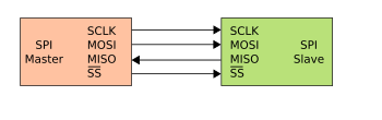
The MOSI, SCK and SS signals are directed from Master to Slave whereas the MISO signal is directed from Slave to Master. The following diagram represents this interface having single Master and single Slave.
SPI Bus – Single Master Single Slave Click to Enlarge
Thus, it should be noted again that during each SPI clock cycle, a full duplex transmission occurs as follows–
Master sends a bit to the MOSI line; Slave reads it from the same line.
Slave sends a bit to the MISO line; Master reads it from the same line.
Multiple Slaves – Slave Select SS Signal
As mentioned earlier, SPI can be used to connect one Master to multiple Slaves as well. Having multiple Masters is also possible, but it does nothing but increase the complexity due to clock synchronization issues, and is very very rare. Having multiple Slaves is where the Slave Select SS signal comes into effect.
SS which means SS complemented signal is in active low configuration i.e. to select a particular Slave, we need to provide a LOW signal level to SS of the Slave. The SPI bus interface is pretty simple for this one, and is shown in the diagram shown below.
SPI Bus – Single Master Multiple Slaves Click to Enlarge
All the Slaves share the same MOSI, MISO and SCK signals. The SS signal is responsible for choosing a particular Slave. The Slave gets enabled only when its input SS signal goes LOW.
In the above case, each of the Slaves is independent since they are separately selected via independent SS signals from the Master. However, there is another way to link the Slaves together – by using Daisy chain configuration. In this configuration, all the Slaves are selected at a time, and the output of one Slave goes to the input of another Slave, and so on. However we will not be discussing this here and in upcoming posts as well since most of the applications don t require this type of configuration.
Keeping synchronization in mind, Master s role doesn t end with simply generating clock pulses at a particular frequency usually within the range of 10 kHz to 100 MHz. In fact, Master and Slave should agree on a particular synchronization protocol as well, or else everything will go wrong and data will get lost. This is where the concept of clock polarity CPOL and clock phase CPHA comes in.
CPOL – Clock Polarity: This determines the base value of the clock i.e. the value of the clock when SPI bus is idle.
When CPOL 0, base value of clock is zero i.e. SCK is LOW when idle.
When CPOL 1, base value of clock is one i.e. SCK is HIGH when idle.
CPHA – Clock Phase: This determines the clock transition at which data will be sampled/captured.
When CPHA 0, data is sampled at clock s rising/leading edge.
When CPHA 1, data is sampled at clock s falling/trailing edge.
This results in four SPI modes, shown in the table below taken from the ATmega32 datasheet page 139. We will discuss more about these modes and how to choose them in our next post where we will learn how to program the SPI of the AVR.
We can also look into the timing diagrams provided in the same page of the datasheet. By now I guess you should be able to decode the timing diagrams yourself. Don t worry about the DORD setting at the bottom, we will discuss about it in the next post. Just focus on what effect CPOL and CPHA has in these figures.
SPI Transfer Format with CPHA 0 Click to Enlarge
SPI Transfer Format with CPHA 1 Click to Enlarge
The In-System Programming ISP exploits the technique of SPI to transfer the hex code from the PC to the target AVR microcontroller. We won t go into the details of how it happens. Since we are discussing about SPI, I thought to bring up this small point as well. The following figure taken from AVR Application Note 910 page 2 shows the simplified hardware connections.
Connections between ISP and AVR MCU Click to Enlarge
This means that if you have connected some SPI device to your AVR microcontroller, and at the same time you are trying to program your microcontroller, there could be some issues like driver contention. We will discuss about this issue and other hardware considerations in our next post.
You might be interested in reading the following documents–
Motorola s SPI Block Guide v03.06
Let s look at what we have learnt in this post.
SPI is a full-duplex synchronous serial data transfer protocol.
Data transfer takes place in between Master and Slave devices.
Each Master/Slave device has an internal 8 bit shift register, which is connected to other devices so as to form a circular/ring buffer.
At each clock pulse, data gets right shifted in the circular/ring buffer.
After 8 clock pulses, data is completely exchanged in between devices.
SPI bus consists of four wires/signals – MOSI, MISO, SCK and SS.
When we connect more than one Slave devices, then we choose them using the SS signal.
CPOL and CPHA must be set so that Master and Slave devices sync properly.
AVR ISP uses SPI to program the microcontroller.
So this was all about the basics of SPI. If you want to know about the pros and cons of SPI, I would suggest you to read this Wikipedia section. In the next post, we will learn how to implement SPI in an AVR microcontroller. So subscribe to stay updated. And don t forget to write your views about this post below.
Cheers. And it s about to be Thanksgiving time in two weeks, so Happy early Thanksgiving. :
Serial Peripheral Interface is a synchronous, full-duplex protocol. SPI is also known as 3-wire interface protocol because it needs 3 communication lines named.
- The Serial Peripheral Interface SPI bus is a synchronous serial communication interface specification used for short distance communication, primarily in embedded.
- Introduction. Serial Peripheral Interface SPI is an interface bus commonly used to send data between microcontrollers and small peripherals such as shift registers.
Serial Peripheral Interface – SPI Basics. Hey all. It s time to continue with our tutorials on serial communication. Till now, we have covered the following.
